
Objective
Data transferring can be supplied by using wireline
and wireless systems. In our project we need to use one of the wireless data
transfer type that is RF data transfer system. Our project is based on the data
transfer that has both transmitter and receiver part called transceiver. The
main objective of this project is constructing the system that transfers the
information (this is text in our project) from one computer to another computer
by using circuit. The communication between these two computers could be
supplied by using transmitter and receiver part with the distance at least 5
meters. Transmitter and receiver part include modulation, demodulation, power
amplifier, antenna and filter.
1. Introduction
While we was
designing this project, circuit was divided into two parts in basically.
Transmitter Part
In
order to transmit a data from one computer to another computer, firstly data
must be converted to electrical signals. Since these signals have low power, transmitting
is difficult by itself. That’s why message signals are required to be modulated,
after this process obtained new signal is converted to RF waves by using loop
antenna.
Receiver Part
Transmitted
data are received by another loop antenna and then demodulation process must be
applied in order to obtain message signal, since these message signals have not
enough power to perceive, amplifier circuit must be used for this process.
Finally message signals (electrical signals) are converted to binary data by using
TTL 232.

Figure 1: Block Diagram of RF Data Transceiver
We have encountered some problems when we are
designing this project. Some of them are listed below.
· Setting Antenna
While electrical signal are converted into RF wave,
we must use loop antenna. However our loop antenna did not work during transferring
process. There were some reasons, main reason was that designed antenna circuit
was wrong, second factor was that since common supply voltage was used, coupling
effect occurred. In order to remove this effect, we tried to use a capacitor
but this element did not work properly. Last reason was that we did not adjust correct
number of turn of the cable.
· Setting Modulation Circuit
Since
we used and gate for modulation process, frequency of signal decreased to 2
MHz. However according to modulation rule, this frequency could be around of 4
MHz .By the end of effort, we have overcome this frequency decreasing. Our
problem was because of the oscilloscope’s time division part. When we put our
message signal on the modulated signal there were perfect matching
· Adjustment Carrier Voltage
In our first design of the local oscillator
circuitry, our carrier voltage was found around 2.5 V. However this voltage was
not sufficient for modulation process to get true result because this is near
the high and low level transition points (low level=2.2-high level=2.5V). That’s
why we tried to increase to nearly 5 V.
1.1 Serial
Data Transmission
Data
tranmission which is physical transfer of data from a point to a point in
channel. There are two ways of this system.One of them is parallel data
transmission ,the other is serial data tranmission.Bits are sent one by one for
serial way.Advantages of serial transmission is that error rate is less than
parallel and transfer rate may be faster.This way can be used for long distance
by adding a check bit (parity bit).In this project, we used TTL 232 cable for
serial transmission.Thanks to this cable ,we got message signal and message signal
was transferred to modulation circuit.This cable has six pins and 9600 baud
rate .
1.2 Crystal Oscillator
Oscillator
which is an electronic device, produces square, triangle and sine waves. We had
to use oscillator to design modulation circuit because carrier signal is
necessary for modulation. Oscillator is a way to generate a carrier signal.
Although there are many kinds of oscillator devices, we used crystal oscillator with
Schmitt Trigger circuitry. We could use crystal oscillator which helps us to produce
high level frequency oscillator circuitry. Operating frequency was 10 MHz for
our project but when we need an amplifier this carrier causes some problems in
bread board. So we should change it with lower frequency than we obtained 4 MHz
carrier frequency.
1.3 Modulation and Demodulation
Modulation and demodulation part
was the most important in our project
since message signals have low frequencies.Modulation technique was developed
in telecomunication in order to send message signal.In generally modulation
process is multiplying message signal with carrier signal because message
signal does not transfer itself without carrier signal. Frequency of message
signal is increased to high frequencies with modulation.There are two types of
modulation techniques.One of them is amplitude modulation and the other is
frequency modulation. In this project, we used amplitude modulation namely we
changed amplitude of message signal with carrier signal because amplitude
modulation and demodulation is easier than frequency modulation and
demodulation.At the end of this process, we obtained modulated signal with
amplitude variations as carrier signal ( in terms of frequency). General
amplitude modulation equation is below .
c(t)=Ac*cos(2*pi*fm*t) s(t)=Ac[1+ka*m(t)]cos(2*pi*fc*t)
-c(t) is carrier signal. -s(t) is modulated signal. -ka is modulation index.
-Ac is amplitude of
carrier signal. -m(t) is message signal.
In this project,we
used and gate (74LS08) for modulation actually there are more than one
tecnquies.However we prefered this method since operating frequency was 4 MHz
and the most optimal device was and gate for this frequency.At the same
time,that was the easiest way.Demodulation which is a way of getting message
signal from modulated signal.We used envelope dedector for this process. This
device includes a capacitor ,a resistor and a 1N4148 diode. Again there are
more than one ways but the technique was the easiest .
1.4 Antenna
Antenna that is a
electronic device , takes electrical signal and converts to RF waves or vice
versa.There are many kinds of it.That’s why we have chosen the simplest way for
antenna since the complexity increases with the distance proportionally. For
our project , straight copper wire was necessary because if the current flows in a wire, magnetic field
is generated and so that radio waves occur in magnetic area.However our antenna
circuit did not work properly so we obtained very weak signal and noise always
interferenced into signal.
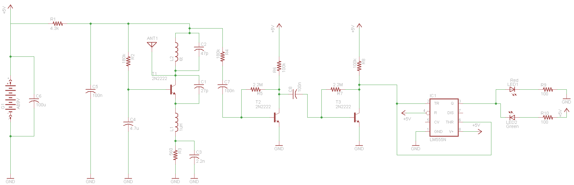
2. Technical Description
RF data
transceiver project depends on two main parts, one of them is transmitter part,
the other is receiver part. These two parts connected each other with two loop
antennas each one of them in one part.
In the
transmitter part, the first process is transferring data from computer to the
serial data transfer system that could be supplied by RS 232 .The data coming
from RS 232 with the TTL level which means analog data comes from the cable[1]. To send and receive signal with
computer we used Serial Port Terminal V1.1 which is easy to use for this
project. After serial data comes as message we need modulation process.
Modulation processes supplies us to transfer data efficiently during the
process, but we need the high frequency oscillator to send message throughout
with channel. Firstly we obtained the frequency 4 MHz frequency and to supply 4
MHz carrier frequency we used Schmitt trigger and 4 MHZ crystal. Output of the
local oscillator circuit, we had 4 MHz carrier signal that is ready for
modulation process. After obtaining the
carrier signal we modulate signal by applying and gate 74LS08 which supplies us
4 MHz modulated signal and sending modulated signal via our antenna which will
be explained in the coming part. Block diagram (under) basically shows the
parts that needs to be completed in transmitter part.
Figure 2:
Block Diagram of Transmitter
After signal sent throughout transmitter antenna, receiver antenna takes
the signal. Modulated and transmitted signal has weakened also some noise added
to the original signal. Firstly we applied power amplifier because this signal
loss some power because of wireless transferring and our amplifier increases
voltage from 40 mV to 4,6V without any problems. Then we applied to envelope
detector to the coming signal. Envelope detector works to detect message signal
with specified capacitance and resistance values. Besides envelope detector
also helps us to decrease effects of the noises comes from the other devices
and noise sources. After envelope we
send data to RS 232 TTL and read message by computer.

Figure 3: Block Diagram of Receiver
2.1 Local Oscillator
Modulation is the most
important part during transmission time, there are two signals that we need.
One of them is message signal and the other is carrier signal in order to modulation.
There are a few ways to generate carrier signal. Our method is crystal
oscillator with schmitt trigger circuitry. We could use crystal oscillator
which helps us to produce high level frequency oscillator circuitry. Oscillator
circuit’s output that we created, is an input of modulator. For this project,
carrier signal frequency is 4 MHz. Because after 20 MHz cosmic noises effects
our signal also 4 MHz carrier frequency was not so hard. So we obtained our
carrier frequency 4 MHz. Also we obtained message signal’s frequency around 9.6
kHz. So this is an amplitude modulation and bandwidth is 2*Fm=19.2 kHz. In our
local oscillator circuitry, at the output we generated 4 MHz sinusoidal carrier
signal. [2]

Figure 4: Local Oscillator
2.2 AM Modulator

Figure 5: Modulator
Modulation
is indispensable for transmission line, since message signals have low
frequencies in order to send these low frequencies some ways have been
developed in telecommunications. In this project we used amplitude modulation
technique. According to this method, in order to transmit message signal, a high
frequency signal is needed thaht is supplied with local oscillator circuitry. During
modulation process, carrier signal and message signal must be multiplied since message
signal has low frequency around 9600 Hz. There are a lot of ways to modulation
we choose and gate 74LS08 which is good for basic multiplication. [3]
2.3 Loop Antenna
Antenna was the most
important part of our project, because we spend almost half of our time to
design a suitable antenna to transmit our data to the receiver part. In first
try, we tried to send data with 10 cm cable but we couldn’t send any data. In
the second try, we established R-L-C circuit also we couldn’t be successful
although we calculated the value of the components as in the second report. At
our third trial we connected our 5V supply in both transmitter and the receiver
part, in this trial we observed the message signal at the end of the receiver
output. But this was not a real transmission, this was just coupling effect so
this was not a successful method. In last try, we turned to coil as inductor
and paralleled 100 nF capacitor we observed some signal at the receiver but
when we amplify this signal we couldn’t get a square wave .So we couldn’t be
perfectly successful but we could send some data which is not noise or
something like that because the shape of output were similar with expected.[4]
2.4 Envelope Detector
Envelope detector
is an important part of the RF data transceiver project. Because modulated
signal transferred to the unmodulated signal which is original message signal given from
the transmitter computer. Envelope detectors designed as a half wave rectifier.
Because when voltage increases capacitor charges, when voltage decreases
capacitor discharges through to the resistor. Advantages of the envelope
detector are cheap and easy to apply and set up. Disadvantage of envelope
detector is decreases the voltage level. To eliminate this disadvantage we
applied amplifier before this process. Also envelope detector are used as
low-pass filter so this helps us to eliminate noises that was added to
modulated signal in the transmission. We can calculate as;
Fc=1/(2*π*(R*C))
Fc is the carrier frequency
Fc=4
MHz , R=40k , C=10pF

Figure 6: Envelope Detector
2.5 Amplifier
During
transmission, because of the channel and the other effects signal’s power
decreases. This weakness causes to unidentified signals coming from the transmitter.
To solve this problem and not to change frequency of the demodulated signal we
need a good amplifier method. For this reason we used amplifier circuit with
the transistors. Because transistors are suitable for working in the sensitive
frequency value. With 2 serial amplifier circuitry we can increase the voltage
from 40 mV to 4.6V. Which is enough to send it to the serial line transmission
part.

Figure 7: Amplifier[5]
3. Test Results
3.1 RS232 TTL Cable Test Results
RS 232 serial port terminal cable’s output values are masured as;
Logic
|
Voltage
|
Frequency
|
Logic 0
|
0.1V
|
0
|
Logic 1
|
5.1V
|
9600 Baud rate
|
3.2 Local Oscillator Test Results
To produce a carrier signal we used 74HC14 Schmitt
trigger circuit and get these results.
Vmax
|
Vmin
|
Vp-p
|
Frequency
|
4.5V
|
-0.4V
|
4.9V
|
10 MHz
|

Figure 8: Carrier Signal
3.3 Modulator Test Results
And gate is the device that runs modulation
process, has some important values for our circuitry
Carrier
Frequency
|
Message
Frequency
|
Carrier
Voltage
|
Message
Voltage
|
Modulated
Signal Voltage
|
Modulated
Signal Frequency
|
10 MHz
|
4.8 KHz
|
4.9V
|
5V
|
2.72
|
10MHZ
|

Figure 9: Modulated Signal
3.4 Receiver Antenna Test Results
At the output of receiver antenna we get;
Frequency
|
Voltage
|
3,98 MHz
|
1,2V
|
3.5 Receiver Amplifier Test Results
When the signal receives the antenna it need to be amplified. To be able
to apply amplifier to the received signal we need a good designed amplifier
circuitry specified to this frequency value.
Input Voltage
|
Output Voltage
|
1,2 V
|
6V
|
3.6 Demodulator Test Results
At the envelope detector’s output we had;
Voltage
|
Frequency
|
3.56 V
|
4.8 KHz
|

Figure 10: Demodulated Signal
No comments:
Post a Comment